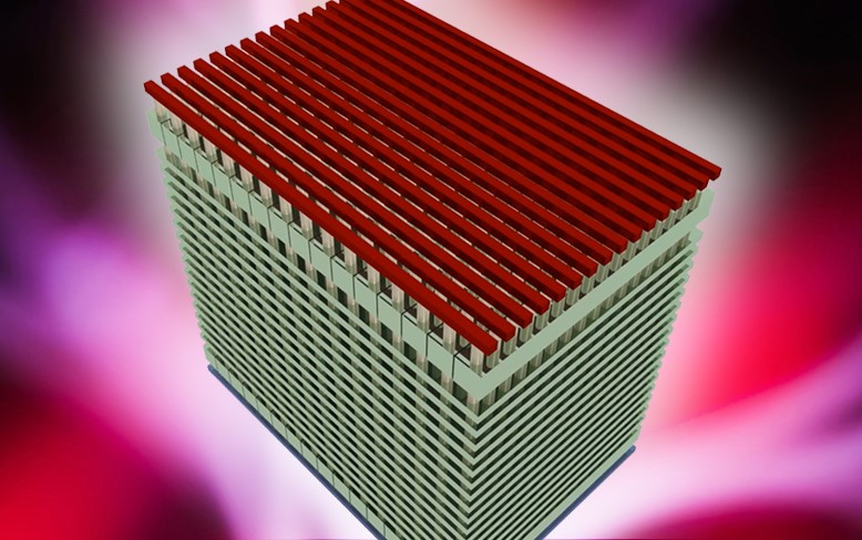
Think of it as a layer cake. We call it BiCS FLASH - and it’s the industry's first 48-layer 3D Flash memory. It’s based on our leading-edge stacking process that surpasses the capacity of the single-plane chips currently used. The process? We stack 48 layers of microscopic NAND layers atop one another – and more layers mean more data. Sounds delicious, right?
The result is good news for consumers: higher capacity storage applications that consume less power, including SSDs, smartphones, tablets, and memory cards. Enterprise SSDs for data centers will get a boost as well.
Toshiba’s BiCS FLASH supports the storage market’s appetite for ever-increasing densities – with the added benefit of enabling innovative designs.
We invented NAND Flash Memory more than 25 years ago – and we’ve been cooking up innovations ever since.
Disclaimer
The views and opinions expressed in this blog are those of the author(s) and do not necessarily reflect those of KIOXIA America, Inc.